《TAIPEI TIMES》GlobalWafers secures direct US funding

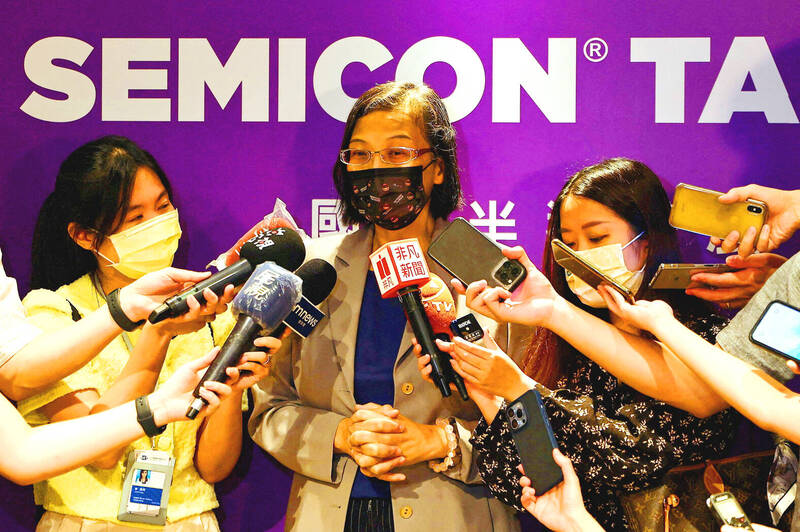
GlobalWafers Co chairwoman and chief executive Doris Hsu talks to media at a Semicon Taiwan event in Taipei on Sept. 13 last year. Photo: Ann Wang, Reuters
INVESTMENT: The company’s planned complex in Texas would be the first 12-inch silicon wafer fab built in the US in more than 20 years, a GlobalWafers official said
By Lisa Wang / Staff reporter
GlobalWafers Co (環球晶圓), the world’s No. 3 silicon wafer supplier, yesterday said it secured up to US$400 million in direct funding from the US Department of Commerce under the CHIPS and Science Act for the construction of two new advanced fabs in the US.
Its subsidiaries GlobalWafers America and MEMC LLC are to build a 12-inch silicon wafer fab in Sherman, Texas, and another one in Missouri to produce silicon-on-insulator (SOI) wafers used to make leading-edge chips.
“With the support of the [US President Joe] Biden Administration, we are honored to be bringing to American shores the world’s most cutting-edge 12-inch semiconductor wafer technology, filling what the White House has called a ‘key vulnerability’ within the US semiconductor supply chain,” GlobalWafers America president Mark England said in a statement.
“GlobalWafers is fully committed to the US market, and we are excited to be playing a defining role in the nation’s semiconductor rebirth,” England said.
When completed, the Texas complex would be the first 12-inch silicon wafer fab built in the US in more than 20 years, he said.
The Texas facility is on track to ramp up volume production in the first quarter of next year, GlobalWafers said.
The new fabs would play a critical role in enhancing the resilience of US semiconductor supply chains, as they would supply US chip designers with domestic wafer capacity to make leading-edge chips for artificial-intelligence (AI) applications or to produce silicon photonics devices used in next-generation packaging technology, GlobalWafers said.
GlobalWafers would reduce the US’ complete dependence on overseas manufacturing facilities, the company said.
The planned 12-inch SOI facility in Missouri would be the first 12-inch fab based in the state when it is completed, the company said.
MEMC is operates an 8-inch SOI fab in Missouri.
The US government funding would be “greatly helpful” in elevating competitiveness of its US fabs, GlobalWafers chairwoman Doris Hsu (徐秀蘭) told a virtual media briefing yesterday, adding that US manufacturing costs tend to be much higher than in Taiwan.
The US$400 million grant would account for about 10 percent of the company’s overall investments of less than US$4.8 billion, Hsu said.
In addition to the direct grant announced yesterday, GlobalWafers plans to apply for the US Department of Treasury’s Advanced Manufacturing Investment Credit of up to 25 percent of qualified expenditures of its subsidiaries, Hsu said.
The US federal funding would comprise one-third of the company’s investments in the two US fabs, Hsu said.
GlobalWafers has secured long-term supply agreements from US customers, including GlobalFoundries Inc, to fill about 80 percent of its planned capacities at the Texas and Missouri facilities, Hsu said.
新聞來源:TAIPEI TIMES


